
In this chapter we will be looking at the basic rules of electricity and the use of basic electronic components so that we have a background for the labs ahead.
Ohm's law relates voltage, current and resistance together as shown by the formula below:
V=IR where: V = voltage (volts or V)
I = current(Amperes, Amps, or A)
and R= resistance(ohms or [[Omega]])
The examples below illustrate the use of Ohm's law.
1. What is the resistance of a soldering iron that draws 0.833A at 120V?
R = V/I = 120/0.8333 = 144 ohms
2. A toaster with 8.27 ohms of resistance draws 13.9A. Find the applied voltage.
V = IR
= 13.9 X 8.27
= 115V
Forcing electrons to flow through a wire against some resistance requires energy. The power used is defined by the formula below:
P = V I where: P = power (watts or W)
V = voltage(volts or V)
and I = current(Amperes, Amps, or A)
By replacing V or I in the power formula with its ohm's law equivalent two alternate expressions can be derived:
P = I2 R and P = V2/R
Examples
1. What is the greatest voltage that can be applied across a 1/8 W, 2.7Mohm resistor without causing it to overheat?
P = F(V2,R)
V2 = PR
V = R(PR)
=R((2.7X10⁶)(1/8))
= 581V
2. A computer chip has 10 outputs which can each provide a maximum current of 100 mA at 5V. How much power is required to drive the outputs if they are all outputting 100 mA?
Total Current = 10x100mA = 1A
P =VI
P= (5)(1)
P= 5 watts
3. What is the cost of operating a car warmer and block heater for 24 hours given a rating of 750 watts each? (Power rate is 10 cents per kw hour.)
= (750+750) watts x 24 hrs
= 1500 watts x 24 hrs
= 1.5 kW x 24 hrs
= 36 kW hrs
(36 kw hrs) (10cents)
= $3.60
Almost all computers contain the basic components, resistors, capacitors, LEDs, and transistors.
Resistors limit the amount of current that flows through a circuit. Given a fixed voltage then the higher the resistance the less current. The resistance of a resistor is indicated by coloured bands on the resistor.
Each color represent a digit as follows:
Colour Value
black 0
brown 1
red 2
orange 3
yellow 4
green 5
blue 6
violet 7
grey 8
white 9
The first three bands indicate the value of the resistor. For example if the resistor had the bands brown red orange this would mean the resistance is 12x103 or 12 KOhms. Note the third band is used as a multiplier. A fourth band is optional and is used to indicate the tolerance of the resistor as follows:
Color % Tolerance
red 2%
gold 5%
silver 10%
no band 20%
Resistors are also rated by the maximum amount of power they can dissipate without overheating. The most common resistors come in ratings of 1/4W and1/2W.
Example
What bands would correspond to a 5% 22 Kohm resistor? The bands are red red orange gold(22x103).
Light Emitting Diodes are used to indicate the state (high or low) of a part of the circuit. LEDs typically can have up to 20mA of current flow through them before they are damaged. This means that a resistor must be connected in series with the LED to limit the current to below this (10mA). A value of 330 ohms is usually used in the lab.

1) The longer pin should be the most positive.
2) The flat edge on the LED indicates the most negative side.
A capacitor is a device which is capable of storing electrons. In the analogy where water is equivalent to electrons, hose size to resistance, and water pressure equivalent to voltage, the capacitor is equivalent to a bucket. Electrons can be "poured" into the capacitor for later use. It is rated in units of farads(F) and has the following circuit symbol:

If the capacitor is polarized (one side must be attached to positive), this is indicated by drawing one of the vertical bars as curved.
The actual physical shape of a capacitor varies considerably. They all have two pins and typically have a cylindrical body, or a flat disc body.
Note that all devices tend to have some small value of capacitance which can often be ignored.
Transistors are the basic building block for most electronic devices. The transistor has two basic modes:
1) amplifier
2) switch
We will be looking at the switch use of the transistor. In the switch mode, the transistor operation can be summarized as follows:
1) on mode: a high voltage applied to the base allows current to flow from the collector to the emitter.
2) off mode: when zero volts is applied to the base no current can flow between the collector and the emitter.

Transistor Circuit Symbol

In digital circuits, two levels of voltage are commonly used to represent thelogical values of "0" and "1". When the voltage corresponding to a "1" is greater than the voltage corresponding to a "0", the system is called positive logic (as opposed to negative logic). Throughout this course positive logic will be used. Typically, positive 5 volts will represent a "1" and zero volts(ground) will represent a "0".
We can indicate the inverse of something by using the word NOT. So "if it's NOT raining I'm going to the beach" is the inverse of "if it's raining I'm going to the beach ". If we let A="raining" and B="going" to the beach then we could express the former as

or the latter as

Notice that a bar above a symbol is used to indicate a logical NOT.
We can indicate that if either of two conditions is TRUE then we will take someaction by using an OR. For example we could say "If it is sunny OR it is above 20 then I'm going to the beach". Let A = "it's sunny", B="it is above 20" and C="going to the beach". Then we can express the above as C=A+B. C is true(going to the beach is true) if either A OR B is true. Notice the symbol "+" was used to indicate a logical OR.
We can indicate that if and only if two conditions are TRUE then we will take an action by using an AND. For example, we could say "If it's not raining AND it's sunny then I'm going to the beach". Let A="raining", B="sunny", and C="going to the beach". The above expression can then be written as

So if both NOT A and B are true then C is true, otherwise C is false (not going to the beach). Notice that a dot is used to indicate the AND operation.
Two forms of "OR" are used in the English language. One form corresponds to the Logical OR we have already discussed and the other to the exclusive or. An example of the exclusive OR would be "If I'm on a date with Susan OR I'm on a date with Debbie then I'll go dancing". It either of the two expressions are true then the result will be dancing. However if he tries to date both of them the result will likely be a slap rather than dancing. So the result of an exclusive or is true if either of the expressions are true but not both. Let A="dating Susan", B="dating Debbie", and C="dancing". The above can then be expressed as:

The + sign in a circle is used to indicate the logical EOR.
The manipulation of functions which contain expressions which evaluate to only true or false (1 or 0) is done using boolean algebra. In this section we will look at describing functions and then at minimizing them.
The logical operations like OR and AND described above as well as other boolean functions can be expressed in the form of a truth table. The truth table enumerates all the possible combinations of inputs and the result for each of these combinations. For example, the truth table below corresponds to C=A+B (C is true if either A or B is true).

In the truth table, "0" is used to represent false and "1" is used to represent true. If there are n inputs to a table, then there will be 2n rows in the table. In the above example, there are two inputs (A & B) so there are 22 rows.
If you have a truth table already and you would like an expression in terms of the input variables, this is easily achieved. In the case of the truth table above, we would want an expression for C in terms of A and B. We can do this by writing out an expression of the sums of all the rows where C is true. In the above table C=1 for three of the rows. The resulting expression is:

This description covers all the cases where C should equal 1. You could try some of the instances of the table to verify that this is a correct expression for C. We will see in the next section that this expression can be reduced to C=A+B which is the result we expected.
We could also write an expression for C based on all the rows where C is zero. This is left as an exercise for the reader.
In the last section, the expression for C derived from the truth table was much more complex than the expression C=A+B which it is equivalent to. Expressions can be minimized by using the rules of Boolean algebra summarized below:

The process of minimizing a function cannot be described in a cook book manner. Several angles of attack may have to be attempted before the best minimization can be found. The basic rules such as involution, dominance, and complementation will likely be easily applied by the reader. Perhaps the other two most useful rules are imdempotence which allows you to duplicate a term if required and DeMorgans law which lets you alternate between the AND and OR form. The examples below illustrate minimizing functions.
Example 1
Simplify the expression X=D(XTO(DE)+F)XTO(F)
X=DXTO(DE)F+DXTO(E)F Distribution
X=D(XTO(D)+XTO(E))XTO(F)+DXTO(F)F Demorgan
X=DXTO(D)XTO(F)+DXTO(E)Xto(F)+D(xto(F)F) Distribution,Association
X=0(xto(F))+Dxto(E)xto(F)+D(0) Complementation
X=Dxto(E)F Dominance
Example 2
Simplify the expression xto(F)=xto(A)BC+ABxto(C)+ABC
xto(F)=xto(A)BC+ABxto(C)+ABC+ABC Indempotence
xto(F)=BC(xto(A)+A)+AB(xto(C)+C) Distribution
xto(F)=BC+AB Complementation
xto(F)=B(A+C) Distribution
F =xto(B(C+A)) Invert both sides
F = xto(B)+xto(C+A) = xto(B)+xto(C)xto(A) Demorgans
As reductions using the theorems of Boolean algebra are at times tricky, a graphical method of carrying out function reductions was developed by M.Karnaugh which makes logic reduction much easier. The Karnaugh map is shown below for three and four variable functions.

The maps above are organized so that groups like

can be recognized and reduced (to A in this case) visually. To do this the truth table is mapped into the Karnaugh map and then squares of '1's are circled from the biggest square to the smallest square. It is important that the minimum number of circles be used and that the biggest possible squares be used in order to achieve a minimum reduction. When identifying squares, it must be kept in mind that the maps are actually three dimensional as shown below:

Example 1
The truth table on the right has been mapped into the KMap and then the squares of '1's circled. Notice that the number of '1's in a square is always a power of 2.

Writing out the term for each group yields the expression below:

A digital IC (integrated circuit) is a collection of components (transistors, diodes, etc.) called a package. The external connections from the outputs, inputs, ground, and power supply to the package are called pins. These pins are numbered counter-clockwise starting at the notched end of the package viewed from the top. Two common types are DIP (dual in-line package) and flatpack.

TTL
Car engines may be divided into two main families, 4 stroke and rotary, and similarly integrated circuits can be divided into two main families based on differences in manufacturing:
TTL Transistor Transistor Logic
CMOS Complementary Metal OxideSemiconductor
There are other families but only these will be discussed here.
a) TTL is reasonably fast, in that it has a reasonably fast propagation delay which refers to the time it takes to get outputs after inputs are applied. The low cost of TTL devices is also an advantage. TTL has a reasonable noise margin and moderate power dissipation. It also has a wide variety of series or types so that a variety of needs may be met.
b) CMOS is slower than TTL but has extremely low power consumption. This means that these devices do not heat up as much. A CMOS that is warm to the touch is probably blown. CMOS also has a high noise margin so it is good inenvironments such as industrial plants. The statistics in the following comparison relate to CMOS and TTL NAND gate devices:
propagation current per
delay package
TTL | 10 nanosecs (average) | 12 milliamps
CMOS | 60 nanosecs (average) | .4 milliamps
DEVICE NUMBERS
Device numbers of TTL fall into two groups, the 54XX and the 74XX series. This numbering system was originally pioneered by Texas Instruments but is now almost an industry standard.
54XX SERIES
The 54XX series conform to military specifications. They tolerate a temperature range of -55 to +125 degrees Celsius. All IC packages consist ofa chip and a case which encloses it. When used in extreme temperatures, it is important that the chip and case be composed of materials which expand and dissipate heat at similar rates. For these reasons all 54XX packages consist of ceramic cases rather than plastic.
74XX SERIES
The 74XX series are cheaper than 54XX packages because they do not conform tomilitary specifications. They tolerate a temperature range of 0 to 70 degreesCelsius and are generally made of plastic.
< u>TYPES OF TTL (54XX and 74XX)
a) REGULAR - lowest priced
b) LOW POWER - exchanges power consumption for speed (identified with an L inthe device number ex. 74LXX).
c) HIGH POWER - typically gives twice the speed as the regular (identified withH ex. 74HXX).
d) SCHOTTKY - uses twice the power as regular but is about 3 1/2 times faster (identified with S ex. 54SXX).
e) LOW POWER SCHOTTKY - uses about 1/5 the power of regular and is slightly faster (identified with LS ex. 74LSXX).
TTL SUMMARY TABLE
TYPE SPEED POWER
regular times 1 1
low power 1/10 1/10
high power 2 2
Schottky3.5 2
Low power Schottky 1+ 1/5
Values in this comparison are approximate
When output for an IC is said to be a "1" or "0" it is understood that this corresponds to some defined voltage range. For TTL chips a "0" can be as high as 0.8V and a "1" can be as low as 2V. The noise margin in this case is 1.2V.If a noise spike greater than 1.2V hits a circuit it could change a "0" to a "1". The noise margin is therefore the maximum value of noise that a circuit can handle and still function properly. For TTL this is typically around one volt. For CMOS the noise margin varies with the supply voltage. Typically the noise margin is 1 volt when the supply voltage is 5 volts and 2.5 volts when the supply voltage is 15 volts.
The diagram below shows the output of one chip connected to the inputs of two other chips.

The chip on the left is outputting current to drive the other two chips. The output current that the chip can provide is finite and therefore the number of chips that can be hooked up to the output is finite. How many chips can be hooked up to an output?
In chip data books it is specified how much current each input on a certain chip takes. For TTL it is typically 1.6 mA. The books also specify how much current each output can provide. This is typically 16 mA for TTL. So for standard TTL, the number of inputs each output can drive is:
16 mA = 10
1.6 mA
This number is known as the fanout of a chip. It will vary depending on what the output currents and input currents are for the specific chips being used.
If something other than an IC is to be fed from an IC output, then the required current must be found in order to determine if the IC output will be sufficient. Never try to draw more current than the maximum recommended operating conditions specified in the data sheets.
The diagram below shows an inverter (shown by the triangular symbol) with an input signal and an output signal.

The time it takes the output to follow a change in the input is called the propagation delay. The timing diagram below illustrates propagation delay for an inverter gate which is typically 10 nanoseconds for a TTL gate.

STATIC ELECTRICITY
TTL IC's are not as susceptible as other types of IC's to static electricity but care must be taken. Static charges can assume very high voltage levels and can seriously damage TTL IC's. CMOS IC's are even more susceptible to static electricity and should be handled with care. When IC's are purchased in bulk quantities they are packaged in anti-static plastic tubes. For individual use there is a type of Styrofoam which is lead impregnated to eliminate static. Since this is expensive, an alternative is to use ordinary Styrofoam wrapped in tin foil.
Before handling ICs the person should ground himself by touching the metal leg of the desk being used. This is particularly important when the person has just been walking around. Walking on waxed floors has produced voltages as high as 15000 volts. Also, many fabrics commonly used in clothing can generate high static voltages as you move. Some electronics laboratories require that a long wire connected to ground be clipped around the wrist of the person handling IC's. Anti-static floor mats are also sometimes used.
The pins on an IC are delicate and can easily be bent or broken off. New IC's sometimes have the pins splayed out. To correct this hold the IC at an angle to a flat surface so that a row of pins touches the surface. Exert pressure very gently until the pins are at a 90 degree angle to the chip. Repeat this with the other row of pins. With used chips be sure that all pins are straight. If one is slightly bent it will not align with the holes in the protoboard board. If the IC is pushed into the board then this pin will be bent more severely and might break off. If the pin bends outward from the IC, it is easy to see and correct. However if the pin bends under the IC then it is not visible but it is not making electrical contact. If at all possible try not to bend pins because repeated bending and straightening can weaken a pin until it breaks off.
To insert an IC into a protoboard board, align each row of pins over the holes on either side of the gutter. Make sure that the surface of the IC is parallel with the surface of the protoboard board. Press the IC into the board by exerting a gentle even pressure with both index fingers. One side of the IC may go in easier than the other so be prepared to correct by exerting more pressure on the other side. Be sure that the IC is firmly seated on the protoboard board.
To remove an IC, use an IC removal tool if one is available. If it is notavaiable a small flat blade screwdriver is useful. Slip the blade under oneend of the IC and gently pry upward a little. Repeat on the other side. Continue prying gently under each side until the IC is loose enough to remove with fingers. Time and care is necessary because it is just as easy to damage pins when removing them as when inserting them.
Once a circuit has been designed using the methods of chapter 3 it can be built in hardware. In order to do this in an organized and therefore error free manner, a logic diagram is drawn using the proper logic symbols and in turn a connection diagram is drawn. Finally the circuit is built on a protoboard based on the connection diagram. Each of these points will be explained throughout the chapter.
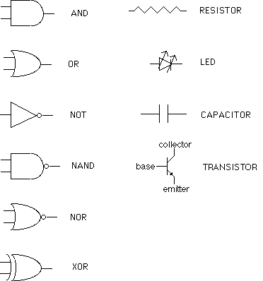
In order to save time when drawing diagrams and make those diagrams easier tounderstand, a standardized set of symbols are used to describe devices like resistors as well as integrated circuits which perform logic functions like AND. These symbols are listed below:
A diagram using the symbols above is called a logic diagram. An example is shown below.
Example
Draw the logic diagram of the circuit needed to implement the function


A logic diagram illustrates the logical operation of the desired system but it does not indicate which pins of the integrated circuits etc. get connected together. A connection diagram is based on a logic diagram but includes the following additional information:
*Pin numbers (it is only necessary to show ground and +5v on one gate for each IC)
*Device numbers
*Portion of an IC used by each gate eg. there are 6 NOT's in a package so one gate would be 1/6
*Any resistors, capacitors, LED's, etc. to be incorporated into the circuit. The values for resistance and capacitance must be specified
Example: Connection Diagram for a Half Adder.

The protoboard is a plastic board that allows circuits to be quickly wiredtogether for prototyping (testing). The protoboard used in the lab is shown below.

Inside the plastic casing of the protoboard (sometimes called a breadboard) are a series of tiny metal clips. A wire inserted into one of the holes in the surface of the protoboard is held in place by one of these clips. Some of the clips are connected together inside the protoboard. There are two rows of clips connected together along the length of the protoboard. This is called the power bus and is sometimes physically separate from the main board. The outside row is generally used for +5 volt connections. The inside row next to the main board is generally used for ground connections. Every IC on the mainboard must be supplied with +5v and ground.
The main board can be logically grouped into 2 parts separated by a groove in the plastic called the gutter. The clips on each side of the gutter are connected in columns but columns are not connected to each other. Also there is no connection across the gutter. The IC is inserted in the board so that the 2 rows of pins straddle the gutter. In this way every IC pin is isolated since there is no connection across the gutter.

IC INSERTED IN PROTOBOARD
Protoboards appear to be quite sturdy but can break if dropped. New boards will be a little difficult to use because the clips have a lot of spring when new. As the board is used the clips will lose their spring gradually and insertion of wires, IC's, etc. will become easier. Trying to force an object larger than an IC pin or resistor lead could cause the clip to be excessively weakened. If a clip does not make good physical contact then there may not be good electrical contact which might cause a circuit to perform erratically.
Be careful in the design process for a test circuit. A beginner's mistake is to rush into implementing a test circuit. However, if the logic diagram is not correct, then the circuit will not work even if the most experienced technician implements it.
1. BEFORE YOU START, draw a reasonably neat connection diagram. Check this diagram against the data sheets carefully to be sure that the pin-out is correct. Many times it is found that a circuit does not function properly because the connection diagram was not accurate.
2. Insert IC's with the number 1 pin to the left side of the board. (the datasheet pin-out shows number 1 to the left.) Be careful not to bend pins but ensure that the IC is firmly seated. A good habit is to connect the IC to the power bus as soon as you have inserted it in the protoboard. Complete the wiring of an IC in a sequence such that the connections which will change most during testing (such as controls) are wired last.
3. Adopt a convention for the power bus. Generally the row closest to the mainboard is used for ground and the outside row is used for +5 volts. Always be careful not to reverse the wires from the power supply.
4. Adopt a color coding convention for wiring. Red is usually used for +5v and black for ground. Data inputs could be one color, data outputs another, and control signals yet another. It is much easier to debug a test circuit if a color code is used.
5. Keep wires short!!! Long wires contribute to erratic operation of test circuits because the amount of resistance and capacitance in a wire increases with the length of the wire. BE NEAT!! A jumble of long wires makes it hard to debug circuits. Moreover, it is easy to loosen or disconnect one wire in a tangle of wires.
6. If wires have to be crossed try to make them cross at right angles. The definition of a capacitor is 'two conductors separated by an insulating material'; which is what is produced in a small way when insulated wires are crossed. Capacitance increases as the area of the conductors in proximity to one another. In the case of crossed wires the smallest area is generated by having them at right angles.
7. Avoid short circuits. Do not strip the ends of wires any more than necessary. Be careful that the leads from resistors and LED's do not make contact.
8. Always protect LED's (not to mention driving IC's) by incorporating resistors in the circuit.
9. If using an unregulated power supply such as batteries:
a) check the power pack voltage level periodically; if the voltage level is lower than TTL recommendations the circuit may still work but will probably perform erratically.
b) use a capacitor across the power supply.
10. Check the connections to each pin very carefully before applying power. If possible allow room next to IC pins so that a logic pen can be used to help debug the circuit. If a circuit does not seem to function as expected do not leave the power connected for extended periods of time. More often than not the problem is in the wiring not in the logic or connection diagrams and prolonged power connection could damage part or all of the test circuit. Disconnect the power, check the wiring carefully against the connection diagram, and if the circuit still doesn't work back up a stage and check the connection diagram. A 'rule' in protoboarding boarding is "blame yourself first -- not the IC".
In chapter 3 combinational design was covered - that is the design of circuits with no memory. This chapter will look at sequential design, which is the design of circuits with memory. Sequential design will let us design much more complicated and useful circuits like counters and even microprocessors. There is a hypercard stack to accompany this chapter which is an animated version of the chapter.
We cannot continue with any theory until we look at the basic memory elements used in sequential design. The most basic is the S-R flip flop shown below.

With an S-R flip flop the S and R signals cannot both be one at the same time. If a '1' is applied to the S input then the Q output will be set (set to '1'). Q will remain set even if the '1' is removed from the S input. Q can be reset to '0' by applying a '1' to the R input. Q will remain at zero even if the '1' is removed from the R input. The reader should try applying a '1' to S and verifying the operation of the circuit.
Quite often we only want the flip flop to be able to change states at certaintimes. For example may have a flip-flop in a house alarm system that is set bya window opening. Thus, setting off the alarm. To prevent the alarm from going off when the alarm system is shut off, we would like to disable the flip-flop when the alarm system is shut off. We can do this by adding some gates to an S-R F/F to make it a gated S-R F/F.

Now the S-R flip flop only responds to the S and R inputs if the GATE signal is high. If the gate signal is low, S and R are ignored.
With the gated S-R F/F we only sampled the S and R inputs when the gate signal was high. There are flip flops that only sample data when the gate signal changes from a low to high (positive going edge of the clock) or some sample when the gate signal goes from high to low (on the negative going edge of the clock).

Notice that the output (Q) only changes when the clock input changes from a zero to a one or vice versa.
In practice S-R F/Fs are not used that often. The most commonlyused flip-flops are the D-flip flop and the JK flip-flop. We will look at each one in more detail.
The D flip-flop (shown below) lets the input at D propagate through to Q on the positive going edge of the clock. The present state-next state chart, shown below, illustrates the behavior of the D flip-flop. Basically Qt+1=D.

The JK flip-flop (shown below) is very flexible and therefore allows simpler circuit designs. Most JK flip-flops allow the signal to change on the negative edge of the clock. The present state-next state chart (shown below ) illustrates the behavior of the flip-flop.

The basic sequential circuit elements necessary to construct sequential designs have now been covered. We can now learn how to interconnect JK flip-flops to make, for example, counter circuits.
The best way introduce you to sequential design is to look at a simple problem:

Trial and error may work for simple cases like this but for larger circuits it will not. We will illustrate the method for larger problems:
LARGER PROBLEM:
Design a counter that follows the pattern below:
 A block diagram of the circuit indicates that there will be three outputs
which correspond to the binary value of the counter and one input to clock
the counter.
A block diagram of the circuit indicates that there will be three outputs
which correspond to the binary value of the counter and one input to clock
the counter.

To implement this we will need three bits of memory. In this example we will use D flip flops. Our circuit will therefore look like the diagram below (minus interconnections between the flip-flops):

The problem that now remains is to determine what to input to the D inputs of each flip-flop. We will start by drawing a Karnaugh map which illustrates the counter operation:
 Note that unused numbers are fed into the proper count sequence.
This way if there is a glitch and the counter gets into one of these unused
states the counter will automatically get back into the proper count sequence.
Note that unused numbers are fed into the proper count sequence.
This way if there is a glitch and the counter gets into one of these unused
states the counter will automatically get back into the proper count sequence.
For each flip-flop we must establish what is to be connected to the D input to have that particular bit count properly. We will look at each bit one at at time. First bit A:
The karnaugh map below shows the transition bit A will undergo for each valueof the counter. For example if the flip flops outputs read 000 then bit A should go from a 0 to a 1 on the next clock pulse.

The above KMap describes how we want flip-flop A to behave. By applying the excitation table of the D flip-flop to the KMap the inputs for Da can be determined.

This is the work to determine the proper connections for the first flip-flop. This procedure must be repeated to determine the proper connections for the other two flip-flops. At this stage the connections look like the following:

The same steps must be applied for flip-flops B and C as shown below:


The final circuit then looks like:

COUNTER DESIGN WITH JK FLIP FLOPS
To illustrate the use of JK flip-flops the design of the counter will be repeated using JK flip-flops. The principals are the same but the excitation table for the JK flip-flop is used (see section 5.4.2)
First bit A:


The completed circuit is shown below (minus clock signal):

The steps used in sequential design are summarized below:
SEQUENTIAL DESIGN STEPS
1) State the problem clearly
2) Draw a block diagram of the circuit identifying all inputs and outputs
3.1) Assign letters to inputs and outputs
3.2) Draw a present state-next state diagram
3.3) For each output draw the Karnaugh maps
3.4) Simplify the expressions for the inputs using the Karnaugh maps
4) Draw the logic diagram
5) Implement the circuit (a connection diagram will be needed if the circuit is to be hardwired)
Up until this point sequential design has been looked at from the perspective of designing counter circuits. By generalizing on what we have looked at so far a wider variety of devices can be designed.
Two flip-flops could be thought of as allowing us to count up to three, or more generally it could be thought of as allowing us to keep track of up to 4 states (states 0 through 3). An example will help:
Suppose someone in the biology department was doing an experiment with rats. In the cage there are two levers; a red one and a green one. Whenever the rat presses the green button twice followed by a red button the rat is rewarded. How would you design a circuit to automatically feed the rat when he pushes the correct buttons? We can do this with the same principles as were used with counter design as long as we broaden how we think about sequential design:
To solve this first draw a diagram representing the various states we have to keep track of:

Notice that each state is represented by a circle and has two arrows leaving the state; one for red and one for green. Each arrow label has the form, input/output. For example, the arrow connecting state A to state B is labelled green/nofood. This indicates that if the input is green the circuit should proceed to state B. While the input is green, the output represents the output of the sequential circuit in state A. It is common that the ouput for a state is the same no matter what the input is.
Since we will implement this using a digital circuit we should convert the diagram to represent things using binary numbers. Let's say every time the rat pushes the green lever, a "1" is inputted into our circuit and every time the red button is pressed, a "0" is inputted to our circuit. When the rat presses the correct sequence of levers, we output a "1" to feed him. Otherwise, our output is at zero.
Instead of calling the states A,B,C and D, we have assigned a number. Note that the assignment of the numbers to the states can be varied (we could call state A 2 if we wanted). The diagram with binary equivalents looks as follows:

Using the above diagram, we can draw a present state-next state diagram to show how the circuit will operate. The state numbers are shown in binary. The least significant bit is labelled A and the most significant B.
Present State INPUT Next State OUTPUT
BA BA
00 0 00 0
00 1 01 0
01 0 00 0
01 1 10 0
10 0 11 0
10 1 10 0
11 0 00 1
11 1 01 1
You can see this is very similar to our counter design except that we do not use the outputs from the flip-flop for driving a display etc. We use the flipflops to keep track of which state we are in.
Similar to counter design we must now focus on each flip flop (on each bit) and complete flip-flop's design. The Karnaugh maps below illustrate this for JK flip-flops:

Since the output is only true in state "3" an AND gate is used to detect when both Qa and Qb are high. For more complex output, criteria a K-map may have to be drawn to determine the relationship between the output and the current state.