Important Information about STM32VLDISCOVERY BOARD
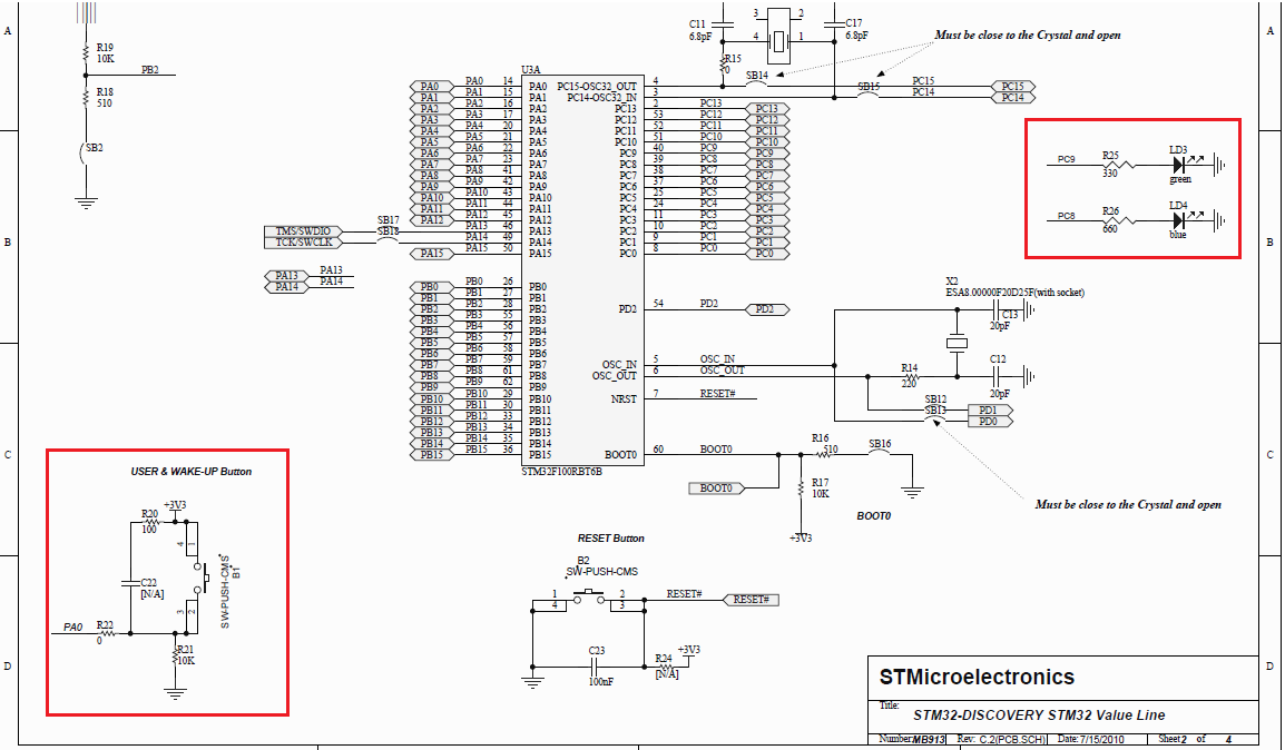
STM32VLDISCOVERY BOARD has two user LEDs (green and blue), so we could manage to make them "blink".
LEDs:
LED1: Red LED LD1 labeled COM indicates communication between PC and ST-Link.
LED2: Red LED LD2 labeled PWR indicats that the board is powered.
LED3: Green LED LD3 labeled PC9 is connected to the I/O PC9 of STM32F100RB*.
LED4: Blue LED LD4 labeled PC8 is connected to the I/O PC8 of STM32F100RB*.
PC[15:0] are mapped to the GPIO Port C, where GPIO stands for General purpose I/O.
GPIO controls hardware peripherals. You must write to registers
that provide information on how that peripheral is to behave.
Do not get these confused with registers from the ARM core!!
In order to write to these registers you must know the address(where they live in address space)
and most importantly what bits to write to these registers.
To know this you must READ the documentation of the registers so you know how they work.
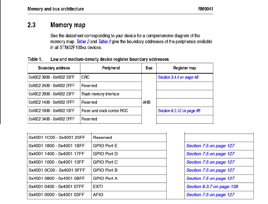
The Boundary address for the GPIO Port C is 0x4001 1000 - 0x4001 13FF from the memory map.
Check the GPIO register bank to get the correct addresses.
Example:
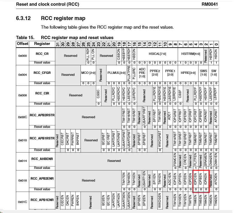
Address of GPIO_CRH (Port Configuration Register for PC15 -> PC8) is given by:
Base Address + Offset = 0x4001 1000 + 0x04 = 0x4001 1004
Wirte the correct value to the GPIO register to activate a GPIO.
e.g. The bit 4 of RCC_APB2ENR (APB2 Peripheral Clock Enabele Register) is set to enable Port C.
Please note that GPIO registers are different from ARM core registers.