Following the notes in the lab, you should have completed the half adder device.
Use the device (the box) and connect binary probes and switches to ensure that the truth table is correct.
Write the boolean functions for sum and carry beside the circuit
Hand-In
- The underlying circuit of the "Half Adder" device. (Circuit with labeled ports--Part 1 in the notes)
- Boolean functions for Sum and Carry
- The "Half Adder" device (the box) with binary switches and binary probes connected to it
(Hint ci+1= the sum of the carries out of the two half adders).
Build and test your circuit with the truth table.
Write the boolean functions for sum and the carry beside the circuit.
Build a full adder device and test it. You will need it to build a 4-bit parallel adder.
Hand-In
- Full adder circuit using two "Half Adder" devices and one additional gate
- Boolean functions for Sum and Carry for the full adder
- The underlying circuit of the "Full Adder" device. (Circuit with labeled ports--Part 1 in the notes)
- The "Full Adder" device (the box) with binary switches and binary probes connected to it
For this, you will use the "Full Adder" device that you just built in the last step.
Test your 4-bit parallel adder device with the following examples:
	  0101 + 0010 = ?
          0110 + 0011 = ?
          and any other examples of your choice
Hand-In
- The underlying circuit of the "4-bit Parallel Adder" device. (Circuit with labeled ports)
- The 4-bit Parallel Adder device testing circuit with the above two examples plus one choice of yours, total three circuits to be handed in.
- Inputs are provided with the binary switches
and the outputs will be displayed with the binary probes.
The Hex Keyboard and Hex Display can be used too.
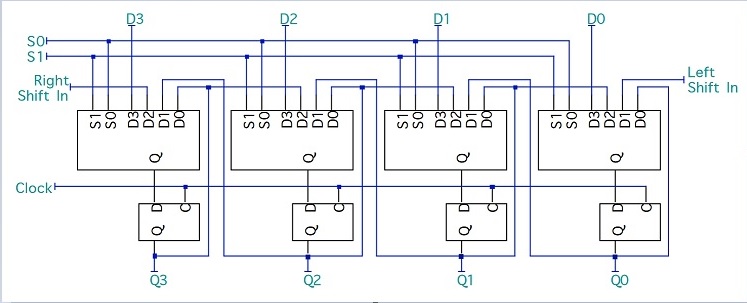
Make sure that you have selection inputs control over it.
	Select Inputs	Function
	S1	S0
	------------------------
	0	0	Store
	0	1	Shift left
	1	0	shift right
	1	1	Load
Here is the design diagram for you:
Hand-In
- The circuit implementing the above 4-bit shift register design.
(Circuit with input/output devices)
Test your circuit with different input values. - The underlying circuit of the 4-bit shift register device. (Circuit with labeled ports)
- The testing circuit of the 4-bit shift register device, the box with binary switches and binary probes connected to it.